RF Packaging, Signal and Power Integrity
The focus of our research lies on the following:
1) Investigation of root causes of signal integrity (SI), power integrity (PI) and electromagnetic compatibility (EMC) issues in RF packages and boards, waveguides and RF front-end modules with integrated antennas up to terahertz frequencies
2) Methods for high-frequency characterization of RF packaging and heterogeneous system integration structures which form segments of signal distribution networks (SDNs) and power distribution networks (PDNs). This includes:
- Die-to-package interconnects, e.g. bond wires, flip chip interconnects
- Power-ground plane pairs with/without decoupling capacitors
- Planar interconnects, e.g. transmission lines in re-distribution layers (RDLs)
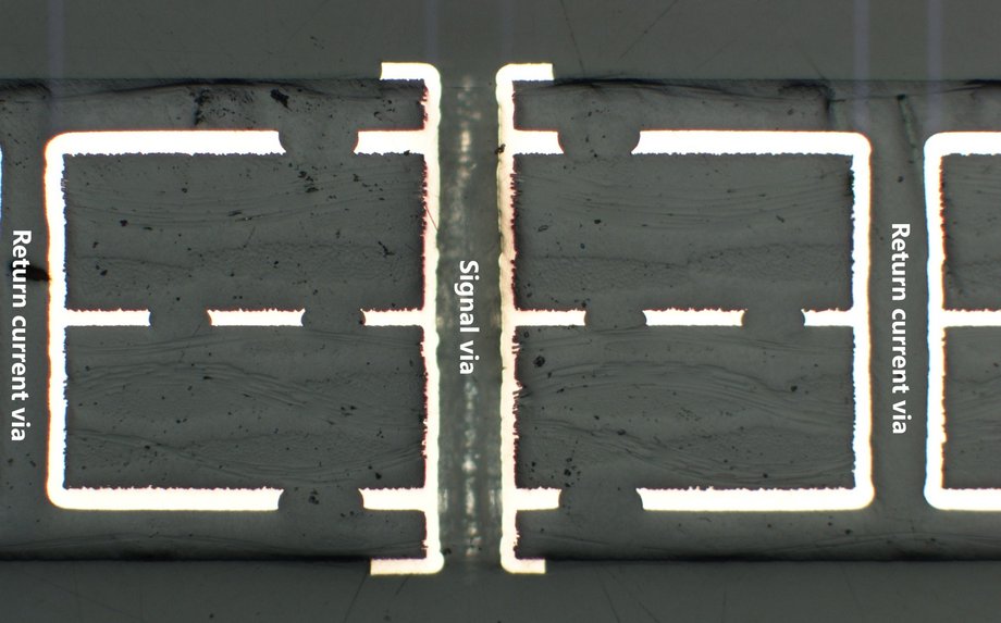
- 3D vertical interconnects, e.g. through silicon vias (TSVs), through glass vias (TGVs), through hole vias (THVs)
3) Methods for electromagnetic modeling, characterization and minimization of:
- Inductance and impedance of PDNs
- Geometrical discontinuities (GDs), reflections and cross-talk in SDNs
- Coupling of simultaneous switching noise (SSN) and electromagnetic interference (EMI) caused by return current path discontinuity (RPD) of vias in multilayered substrates
- Impact of non-ideal effects of RF packaging and system integration structures on SI, PI and EMC
- SI, PI and EMC issues in RF packages/interposers (with high-speed and high-bandwidth links) for 2D, 2.5D and 3D heterogeneous integration of chiplets, active and passive components
- Undesired electromagnetic radiation from electronic packaging and heterogeneous integration structures