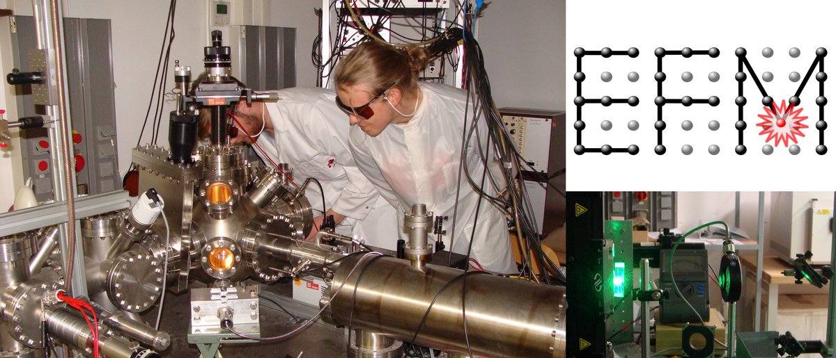
Our research is focused on the development, fabrication and characterization of nano- and optoelectronic devices based on the group-IV semiconductors Silicon, Germanium and Tin. We also explore the use of functional oxides. We combine materials research with the development of novel device concepts with applications ranging from sensors to spintronics. One example is the use of low-dimensional semiconductor heterostructures and metallic nanostructures to develop integrated biosensors. We are one of 12 ForLabs in Germany that have recently been equipped with state-of-the-art processing and characterization equipment to that purpose.
https://www.forlab.tech/ueber-forlab/forlab-famos/
News:
Congratulations to Paul Oleynik for getting the university's Young Researcher Best Paper Award 2024!
https://www.b-tu.de/en/news/article/26808-outstanding-research-achievements-at-btu
Our paper "Strong optical coupling of lattice resonances in a top-down fabricated hybrid metal-dielectric Al/Si/Ge metasurface" was published in Nano Letters:
https://pubs.acs.org/doi/full/10.1021/acs.nanolett.3c05050
Our paper "Influence of material and geometry parameters on resonance linewidths of plasmonic modes in gratings made from highly doped Ge1-xSnx" has been accepted for publication in Journal of Physics D: Applied Physics.