Project description
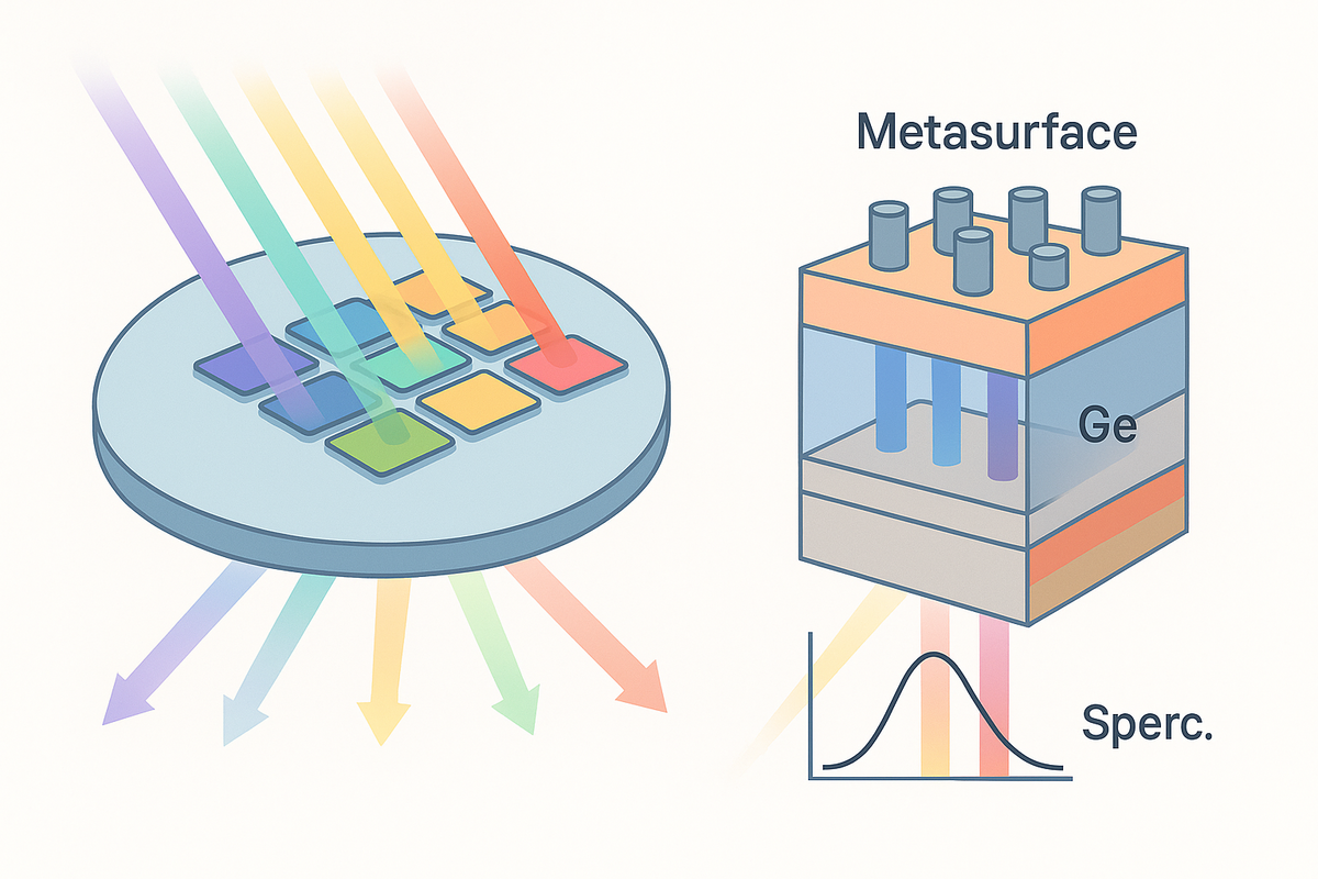
We are developing wavelength-selective photodetectors built from Si/Ge heterostructure metasurfaces—ultra-thin, nanopatterned layers that act like on-chip optical filters and light harvesters at the same time. Each pixel is a vertical Ge PIN diode grown on a silicon-on-insulator (SOI) wafer; the top Si and Ge layers are etched into a periodic “forest” of 400–900 nm pillars. This all-dielectric metasurface traps light at a single, designer wavelength and funnels it straight into the absorbing Ge layer.
Why it matters The metasurface boosts absorption to ≈45 % at 1.4 µm with only a 150 nm-thin Ge layer—performance normally requiring four times the material—while keeping the full width at half maximum (FWHM) only a few tens of nanometres . Because the resonance position shifts monotonically with pitch and pillar diameter, we can lithographically dial any target line between 1.2 µm and 1.55 µm.
Fabrication highlights All structures are made in a single top-down CMOS-compatible flow: epitaxial Ge on SOI, plasma etching of the nanopillars, and a blanket dielectric cap for passivation and future transparent contacts . The Si/Ge/Si stack also provides a continuous, low-resistance contact plane—no tricky nanoscale wiring required.
From pixels to spectrometers By placing 9–25 different metasurface pixels side-by-side, each tuned to a slightly offset resonance, the chip becomes a snapshot spectrometer. A lightweight Gaussian-matrix algorithm converts the set of photocurrents into a 300-point spectrum; the team demonstrates accurate reconstruction of plant-leaf water-stress signatures across 1.3–1.6 µm .
Key advantages
Spectral purity & tunability without external filters
Robustness against etch-depth errors and side-wall angle variations, thanks to the Si/Ge heterostructure design
Seamless integration with silicon photonics and CMOS read-out, enabling low-cost hyperspectral cameras, fibre-optic monitors and environmental sensors.
In short, the project turns a single photodiode into a precision optical filter—then multiplies it into a compact array that delivers full near-infrared spectra on-chip.
Objectives
the main purpose of this project is the reconstruction of sensivity index in the range of different wavelenght by utilizing machine learning methods with available dataset.