Research Topic
Improving Thin-Film Solar Cells by Deliberate Interface Tailoring
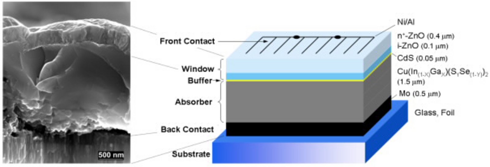
In recent years, thin film photovoltaics have exhibited rapid and impressive development. Today's thin film photovoltaic systems are on the verge ofo commercialization, superseding the (more expensive) current state-of-the-art wafer-based Si solar cell technology. However, the next crucial level of performance can only be reached by knowledge-based optimization, augmenting and accelerating what can be achieved through trial-and-error device improvement. Thin film solar cells are composed of a stack of many thin layers having different chemical and electronic structures. The resulting interfaces can often act as recombination centers when not designed carefully. In most cases, the interfaces are the factor that determines the local electric fields within the device. Thus, the key to continued fast progress is the knowledge of and the ability to deliberately tailor the electronic and chemical structure at the interfaces in such thin film devices.
To tackle the complex and challenging tasks involved in such projects, the Young Investigator Group proposes an interdisciplinary three-pillar approach:
I. Study the performance and the electronic characteristics of the solar cell device.
II. Examine the initial electronic (e.g., band offsets and charge carrier dynamics) and chemical interface structure.
The information gained from I. and II. is used to develop and improve upon models that can describe the "real-world" devices under investigation, with the goal of determining the identities and properties of the performance-limiting interfaces, leading to the final pillar:
III. Recommend and employ deliberate surface/interface modifications to systematically tailor the electronic structure in order to reduce/avoid loss processes.
The goal of the Young Investigator Group is to develop and establish this analysis/optimization approach.